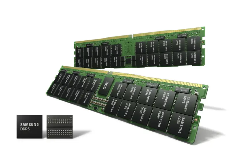
Samsung Electronics is a key player in the electronic market. It has a wide range of products. Samsung is undoubtedly one of the world’s best leaders in the memory technology field. Earlier today, Samsung Electronics started mass producing the industry’s smallest 14-nanometer DRAM based on extreme ultraviolet (EUV) technology.
Samsung has been a pioneer in technology innovations, with the multi-layer EUV that made the 14nm DRAM possible they were able to achieve another milestone. Without the multi-layer EUV, it is not possible to manufacture the 14nm DRAM using the conventional argon fluoride (ArF) process.
With this, Samsung will be able to address the need for greater performance and capacity in today’s digitally growing world. With the scaling of the architecture, EUV technology will become important in the coming days ahead. Samsung was able to achieve the highest bit density while increasing the overall wafer productivity by approximately 20% using the five EUV layers to its 14nm DRAM. Furthermore, the 14nm process aims to reduce the power consumption by nearly 20% compared to the old generation DRAM nodes.
The 14nm DRAM will be able to get the most out of the DDR5 standard and can clock speeds up to 7.2 GB/s. Samsung also plans to expand its 14nm DDR5 portfolio to support various IT fields along with the aim to grow its 14nm chip density to 24GB.